Analog layout – Stop the antenna effect from destroying your circuit
There is a problem at the heart of how ICs are made, which unless carefully managed by the layout designer can destroy the circuit as it is being fabricated.
Integrated circuits are made using an iterative build-up process, many layers of different materials are deposited onto the silicon substrate to create the devices and wires of the circuit. Each iteration of the process deposits a thin layer of new material and then removes the excess by masking and etching, leaving behind the required pattern. In most modern processes the etching is done with a plasma etching process.
The silicon wafer is held in a near-vacuum, and a gaseous etching agent, often a fluorine compound, is introduced into the chamber. The gas is energized and turned into a plasma by exciting the atoms with RF radiation. The plasma creates “free radicals” which are highly reactive compounds that are missing a valence electron. The vacuum chamber also contains electrodes; the ground electrode is connected to the wafer being etched. An alternating potential is applied across the electrodes and the ion flow pushes the free radicals to the surface of the wafer. The free radicals react with the surface material and etch it away.

A major advantage of plasma etching, compared to wet etching, is the ability to get a highly directional (anisotropic) etching process. Deep trenches with near-vertical sides can be etched into the surface of the wafer, allowing the incredibly fine structures of a modern integrated circuit to be created.
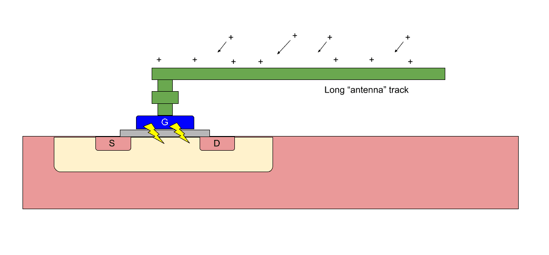
The problem with plasma etching is that it can destroy the devices of the integrated circuit as they are being constructed. Ions formed in the plasma, transfer charge to the wafer being etched. As the layers of the circuit are built up there are situations where a long metal track is only connected to the gate of a MOSFET. These long tracks collect charge from the plasma which is unable to “escape” through the gate oxide layer to the substrate. The oxide layer is often only a few molecules thick, and if enough charge builds up, the thin oxide layer breaks down, damaging or even completely destroying the MOSFET.

This accumulation of charge is usually, and misleadingly, called the antenna effect. In analog design, we aren’t only worried about the complete failure of devices, due to the antenna effect, but also its impact on device matching. Carefully matched devices in current mirrors and differential pairs can be unbalanced if one of the devices is slightly damaged during manufacture.
Each connection on an IC joins a diffusion contact of one device to the gate of another. (In reality, multiple diffusions contacts often connect to multiple gates, but the problem remains the same.) During manufacture, if part of the metal wiring is connected to the gate, but not a diffusion contact, this “floating” metal collects charge from the plasma. Manufacturing rules for the antenna effect are usually expressed as the ratio of the area of floating metal (i.e. charge collection area) to the area of the gate. A larger charge collection area will allow a greater charge to collect on the gate, making oxide breakdown more likely.
To prevent the antenna effect from destroying your circuit you need to reduce the floating metal/gate area ratio or give the charge a safe way to dissipate to the ground before it can build up and cause damage.
To reduce the floating metal/gate area ratio, the layout designer must change the routing so that the highest part of each connection is close to the gate. This will mean that there is a full connection to the diffusion contact before the area of floating metal becomes too large. Sometimes this can be done naturally by completing the connection to the gate on the highest metal layer, and sometimes it is necessary to add jumper tracks into the connection.
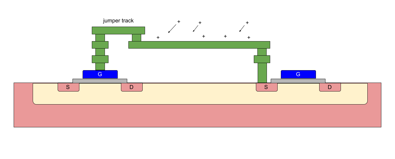
A jumper breaks the long track close to the gate, reducing the charge that can accumulate during fabrication below a safe limit. The jumper is constructed so that the long track is only connected to the gate once it has also been connected to a diffusion contact, which then allows the charge to dissipate through diffusion to the substrate. Jumpers can be used to effectively control antenna issues, but complicate the routing by adding lots of extra vias and small pieces of wire into the layout.

An alternative solution is to place a reverse-connected diode close to the gate. Instead of reducing the antenna effect, the diode allows the charge to safely dissipate to the substrate during fabrication. To make this easy some transistor pcells have an option to add a diode to each gate in the layout. Diodes are a very effective way of preventing antenna effect damage, but the downside of inserting diodes into a circuit is that they add extra capacitance, which affects circuit performance, and they increase area.
As with so many aspects of analog layout, there is no “right way” of controlling antenna effects. The layout designer must balance the tradeoffs in each case.
Interested in adding quality and speed to your design? Sign in to our free webinar below: