Stacked MOSFETs in analog layout
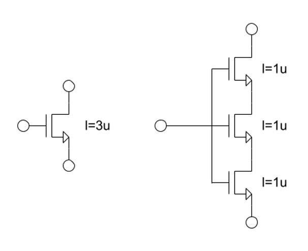
Below 28nm, maximum device length limitations mean that analog designers often need to connect multiple short length MOSFETs in series to create long channel devices. These series-connected devices are often called stacked MOSFETs or stacked devices. For example, stacking three 1um MOSFETs in series creates an effective device with a channel length of 3um.
Stacked MOSFETs are very common in modern analog design but are not without issues. The main problems are increased capacitance and greater area. The increased capacitance is largely due to the increase in interconnect around the devices. The overall gate area and gate capacitance remain similar to the non-stacked equivalent, but there is extra parasitic capacitance on the interconnect. The physical separation of the devices in the stack increases the overall design area compared to a single long-channel device.
When using stacked MOSFETs in a circuit, the layout quality becomes even more critical than usual. Poor layout increases the parasitic capacitance and design area significantly and can result in a circuit failing to meet the desired performance characteristics. Layout engineers must design the layout of such devices with great care. Most designers working at these smaller process nodes have experienced situations where pre and post-layout simulations are very different. Quite often, this is due to the effects of interconnect parasitics on stacked devices.
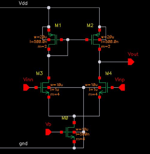
Let’s take a look at a few ways of achieving a high-quality layout for stacked MOSFETs. The subcircuit below shows four nmos MOSFETs that have been stacked together to create a long-channel device.
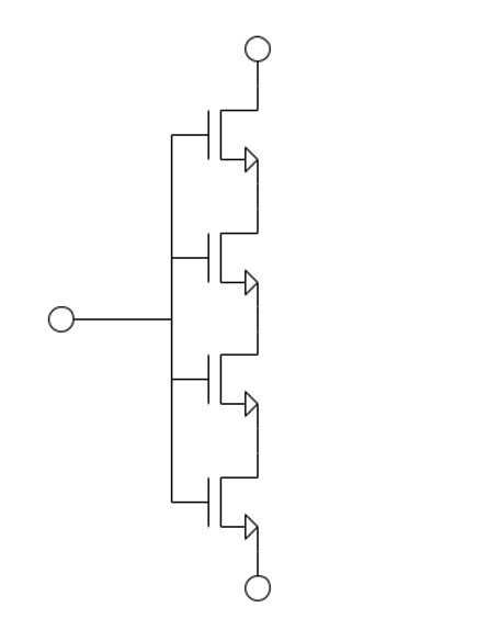
In this circuit, you can see that all the gate pins are connected (as are all four bulk connections); you can also see that the MOSFETs have been connected in series with the drain of one connected to the source of the next. Because, in this case, each device is a simple single-finger MOSFET, we can use a simple diffusion sharing layout pattern when designing a layout for this structure.
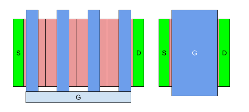
The layout of the simple stacked case is shown on the left of the image above; you can see that there is very little additional interconnect, as the equivalent long-channel device (on the right) would also require a poly contact. The area penalty is significant in this case, but this is unavoidable and determined by the poly min-spacing rule.
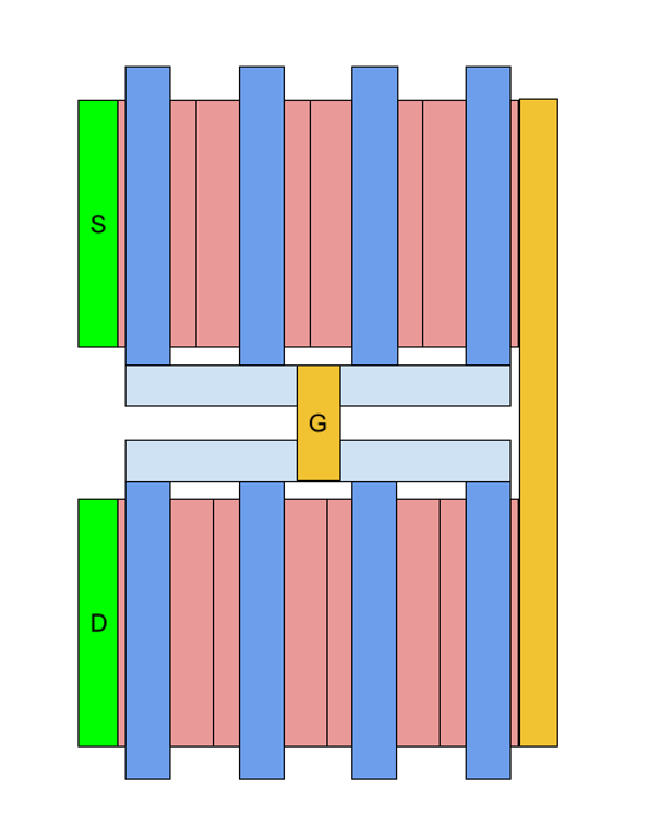
Another problem with this approach is that very long effective devices can result in long chains of diffusion sharing. However, it is possible to fold long chains onto multiple rows, as shown below. The tradeoff is that this adds additional interconnect and further increases the capacitance of the stacked device.
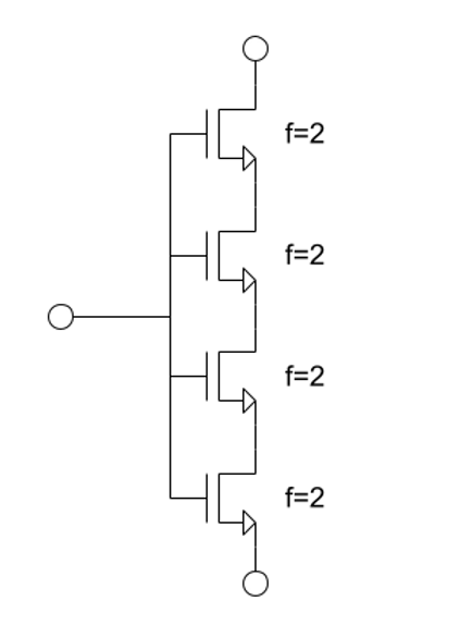
The following circuit shows a case where the circuit designer has wanted to use two finger MOSFETs in the circuit to achieve better matching.
Two finger devices can not be connected by diffusion sharing, so we must use a different placement and routing approach. In order to achieve a compact layout, the devices are connected in columns instead of the row-based pattern shown in the previous example.
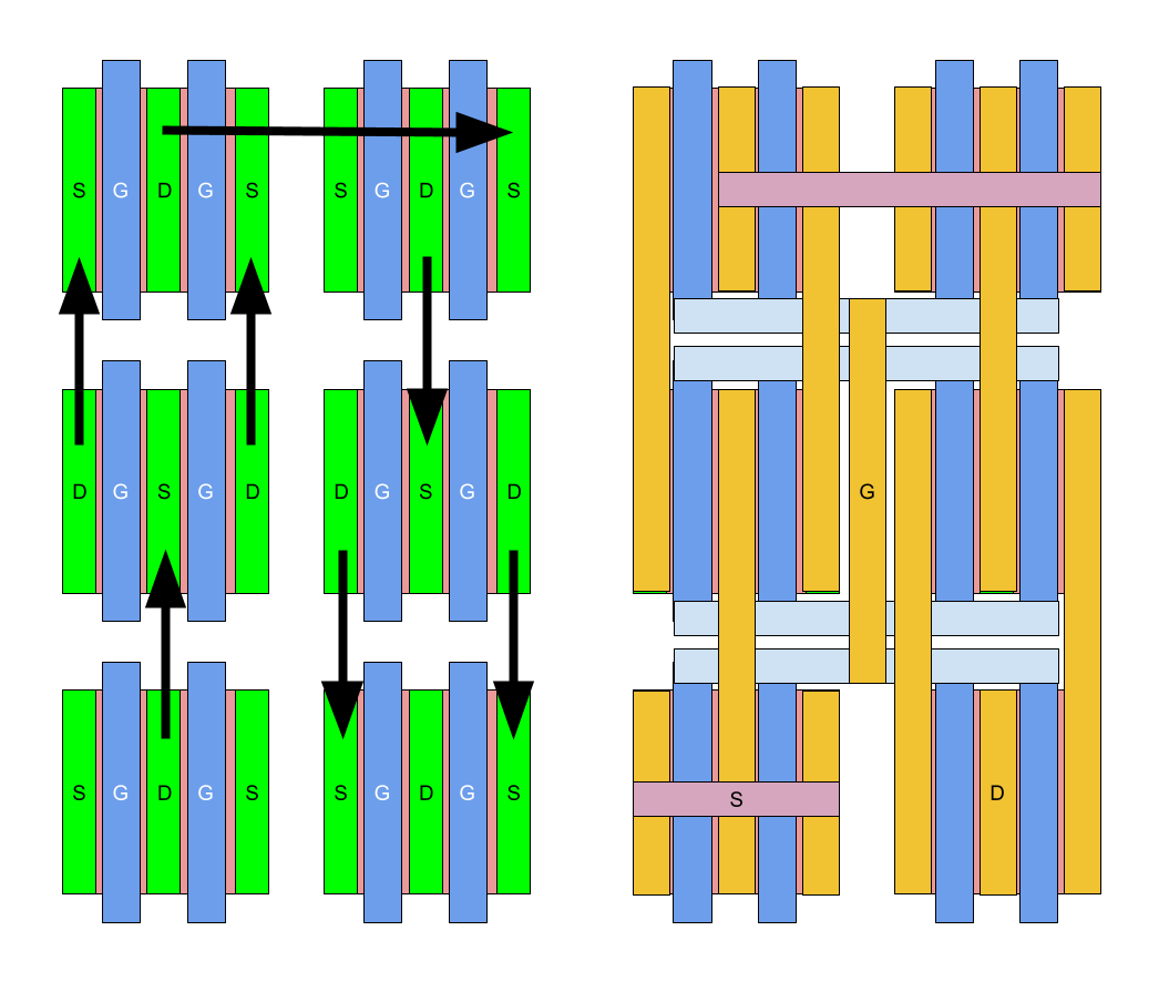
The image on the left shows the connection pattern, the drain of one device connecting vertically to the source of the next. As you can see, the connectivity runs in columns, with alternating devices having different parameters that swap between the drain-center and the source-center variants of the MOSFET. The swapped contacts allow straight-line routing between the devices in the column, avoiding bends and additional vias.
You can see the routing pattern for this column-based pattern on the right. There is additional interconnect, but not significantly more than would typically be needed anyway for contact reinforcement.
The circuit designer might also specify an m-factor for the stacked device. A stacked and m-factored topology allows the circuit designer to build devices with long and wide channels using a number of small MOSFETS. This example shows a single-finger stacked device with an m-factor of 4.

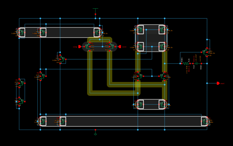
In the layout below you can see that the pattern has four copies of the previous row-based pattern, arranged to ensure the minimum amount of additional routing between the devices.

In this article, I have shown a few of the basic patterns that can be used with stacked MOSFETs. In all of these examples, the placement and routing of the devices are critical in achieving a high-quality layout.
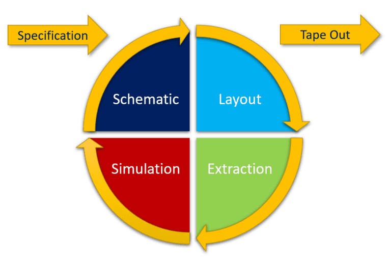
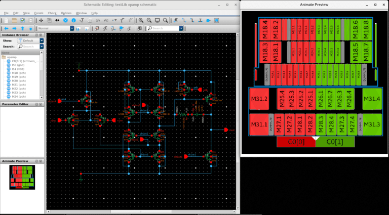
The technology in Pulsic’s new Animate Preview tool combines placement and routing in a single operation. This allows Animate Preview to achieve the type of optimal layout pattern for stacked devices shown above. The exact position, orientation, and parameterization of each device must be optimized to obtain the desired result. At the same time, the tool must consider the current flow through each device so that the interconnect complexity and length are minimized. Analog layout always requires a careful balance of multiple competing priorities; no one way of doing things will work in all cases.
To learn more about Animate Preview and advanced analog layout visit https://animate.pulsic.com