Analog layout – not just transistors
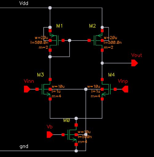
Look at any schematic for a CMOS Analog IC circuit and you will see symbols for NMOS and PMOS transistors as well as resistors, capacitors, and inductors. You will also see the wires joining the symbols together that define the circuit connectivity. At a basic level creating a layout for a circuit is the process of drawing the silicon geometry for these symbols, and connecting them together with wires. In most cases, the geometry of the symbols is defined by parameterized code, in the form of Cadence PCells or iPDK PyCells. Then the connecting wires are usually hand-drawn by the layout designer.
But, in addition to the symbols and wires of the circuit, there are several other structures that the layout designer must create for the circuit to actually work. Some of these additional structures are shown on the schematic, some are added to the schematic later in a process called back-annotation and some structures are never shown in the schematic and their existence must be implied by the designers. Schematic diagrams are not detailed blueprints but are more like architectural sketches for the circuit. The role of the layout designer is to use their training and experience to interpret the schematic to create a successful layout. Let’s take a look at some of these additional structures and the role they play.
Wells, Taps, and Guard rings.
Most CMOS processes are constructed with a P-type bulk substrate and NMOS devices are constructed by implanting N-type source and drain geometry. To construct a PMOS device a region of N-type material is needed. The N-type material is called the N-well and it surrounds the P-type source and drain geometry to create the MOSFET channel. The N-well must be drawn in the layout. It is usually included in the pcell/pycell code, but the layout designer is responsible for extending this region beyond the individual transistors and creating a continuous N-well around a group of devices.
The performance of a MOSFET transistor is very sensitive to the potential of the N-well, and P-type bulk (and on deep N-well processes the P-well). A build-up of charge in the well changes the characteristics of the transistor and must be carefully managed, usually (but not always) by ensuring that the well has a good electrical connection to power for the N-well and ground for the P-well. This connection is achieved by inserting taps and/or guard rings into the layout. A guard is essentially a ring-shaped tap that wraps around the transistors. Taps and guard rings also reduce the likelihood of latch-up, where a low impedance path between the power rails is formed, creating a damagingly high current through the circuit.

PMOS and NMOS devices with taps
In addition to maintaining the potential of the well, guard rings also help isolate sensitive devices from being affected by charge flow and electrical noise from other parts of the circuit. For this reason, guard rings are very widely used in analog design. The typical four-terminal MOSFET schematic symbol specifies the connectivity of the well but the taps and guard ring structures are not drawn on the schematic. Layout designers must know how and where to insert them.
Jumpers and Diodes
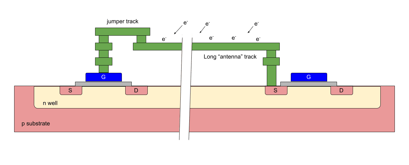
Another example of critical layout structures that don’t appear on the schematic is the insertion of jumpers and/or diodes to protect against so-called antenna effects.
The IC fabrication process involves many iterations of material deposition, masking, and plasma etching. Each iteration adds a layer of material and then removes the excess using a high-energy plasma. As the layers are built up there are situations where a long metal track is only connected to the gate of a MOSFET. These long tracks collect charge from the plasma which is unable to “escape” through the gate oxide layer to the substrate. If enough charge builds up (and therefore potential) on the gate this can cause the thin oxide layer to break down, damaging or destroying the MOSFET. This issue is avoided by adding jumpers and/or diodes to the layout.

Antenna breaking jumper track
A jumper breaks the long track close to the gate, reducing the charge that can accumulate during fabrication below a safe limit. The jumper is constructed so that the long track is only connected to the gate once it has also been connected to a diffusion contact, which then allows the charge to dissipate through diffusion to the substrate. Alternatively, a reverse-connected diode can be placed close to the gate. Instead of reducing the antenna effect the diode allows the charge to safely dissipate during fabrication but has minimal effect on the transistor during operation.
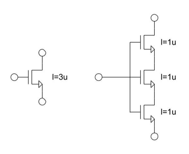
Dummy Devices
Many processes require designers to insert dummies into the layout if they need matching devices. Later processes require dummies at the end of each “row” for all devices. Dummies help ensure that each device in a matching group (e.g. a current mirror) has the same geometry when etched in silicon. Optical distortion resulting from sub-wavelength patterning is minimized by repeated patterns in the layout. Process engineers are able to use techniques such as optical process correction (OPC) to some degree, but it is better to produce a uniformly patterned layout. Where those patterns change, the silicon deviates from the drawn layout the most. By inserting dummies around matching structures layout designers extend the pattern, meaning that the matched devices are inside the core of the etched pattern.
The second reason that dummies help matching is by reducing certain other types of LDE. For example, dummies reduce the well proximity effect, by increasing the distance of the matched devices from the well edge.

Well proximity effect on the device threshold voltage
Dummy devices don’t usually appear in the initial schematic, but unlike the other structures mentioned in this article, once the layout is complete dummies must be back annotated into the schematic. Dummy devices are complete but non-functional transistors and they are detected by LVS tools and must be accounted for.
Circuit engineers can’t rely on schematic simulation alone to verify their circuits. Layout extraction and full parasitic simulation are essential to verify any analog circuit. But, creating a high-quality layout from a schematic is far from being a simple process. This article was a quick introduction to the “other” things that need to be included in the layout of a typical analog block but that are not part of the schematic. All these structures play a critical role in the fabrication, operation, and performance of the circuit.
Next time I will look in more detail at how these structures are implemented in CMOS layout and at some of the tradeoffs the layout designer must consider when incorporating them into the layout design.