Substrate Noise coupling in integrated circuits
Silicon integrated circuits utilize various forms of isolation to electrically isolate devices, such as reverse-biased PN junctions or trench isolation. With the exception of exotic materials such as silicon-on-sapphire, they all utilize a silicon substrate which is a potential path for noise coupling. Such coupling can decrease performance or even cause functional failures. So designers need to use various techniques to reduce noise coupling.
Various different substrate types are typical:
- High resistivity; used for RF where low loss for devices like on-chip inductors and capacitors is desirable.
- P type epi grown on a P+ substrate typically used for digital logic. The combination of low resistivity substrate, giving latchup protection, and higher resistivity epi for device performance is possible.
- Low resistivity buried layers and high resistivity epi for bipolar processes.
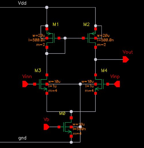
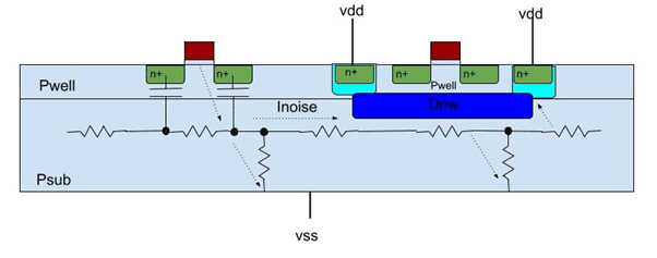
In Fig 1 we show a typical case where there are 2 NMOS devices in a common P type substrate. At sufficiently low frequencies (< 10GHz) the substrate can be considered purely resistive, so noise coupling is primarily through the PN junctions and the substrate itself.
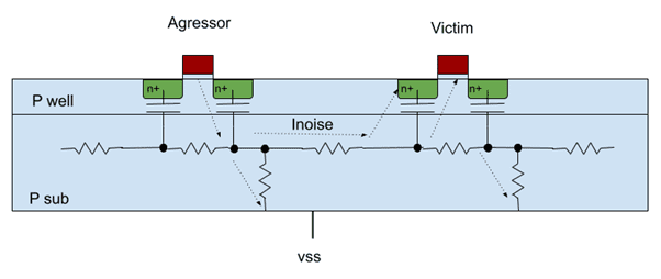
In the above example noise can be introduced into the substrate from a number of sources:
- Impact ionisation in the channel of MOS devices
- Capacitive coupling from noisy signal through the PN junctions
- Package RLC giving rise to supply bounce due to power transients and Ldi/dt effects.
The noise can then travel through the substrate to sensitive areas of the circuit. Typically noise may originate in a fast switching digital block and couple to an analog block. There, the fluctuations in substrate voltage can cause the Vt of devices to vary and cause gain variation. Tools available commercially can analyze substrate noise coupling, typically by formulating an RC mesh of the substrate. Knowing the doping profiles of the junctions and wells, the resistivity of the substrate can be discretized to form the RC mesh which can then be solved using a finite element or boundary element method to solve for voltage and current with respect to time and/or frequency. However, a full analysis is complex and time-consuming, so many designers apply tried and tested techniques to reduce substrate noise issues.
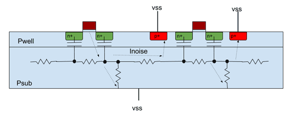
In the simplest case for devices in the P substrate (Fig 2), a P+ guard ring around the sensitive devices and/or around the noise transmitter can reduce substrate noise coupling by 30dB [1].
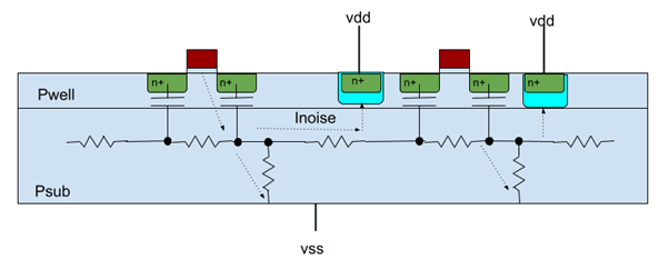
Another approach is to use an NW guard ring tied to VDD to provide a reverse-biased PN junction (Fig 3). This provides somewhat better reduction of noise especially at low frequencies where the impedance of the junction capacitor dominates over the substrate resistivity but uses a larger area.
A third approach uses deep NW to isolate devices in their own P tub giving even better isolation (Fig 4). Care must be taken with the net that the DNW is tied to. At first, it might seem that tying it to VDD is correct, in order to reverse bias the PN junctions. However if it is tied to the common VDD – with supply transients exacerbated by package or bond wire inductance – it will act as a strong noise transmitter into the isolated P well due to the large area junction capacitance. Tying the DNW to VSS, preferably independently of the rest of the chip VSS, can prevent this.
In summary substrate noise coupling is a serious issue with high-speed digital circuitry on the same substrate as sensitive analog or RF circuitry. The coupled noise can degrade performance or even cause functional failure. Careful use of guard rings can help minimize this noise with a small increase in area.
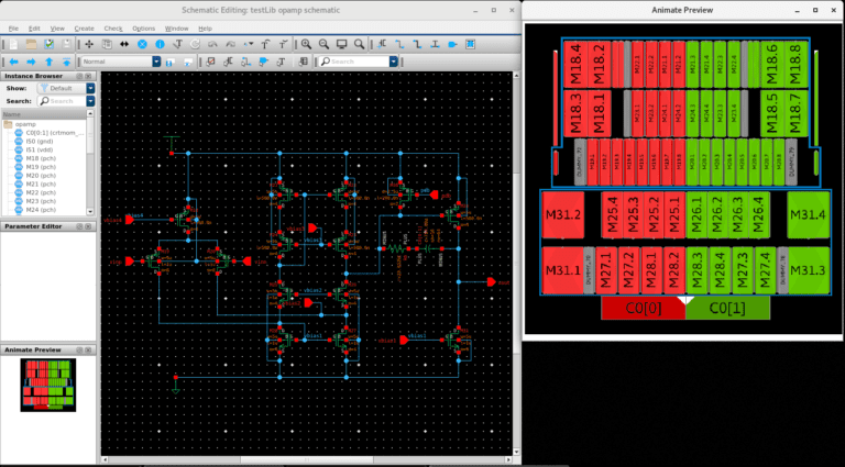
Animate Preview automatically creates guard rings and inserts deep NW to isolate devices from coupling noise. Click here to learn more about Animate Preview or visit https://pulsic.com/animate
References
- ‘Substrate Noise Coupling in RFICs’, Ahmed Helmy, Mohammed Ismail. Springer (ISBN: 978-1-4020-8165-1)