There are key structures that are essential to the working of any MOSFET circuit. The best examples of these are well, taps, and guard rings. Understanding the part that the substrate plays in a MOSFET circuit is critical to creating a working analog design. In order to do this, it is necessary to first understand how a MOSFET transistor works.
Let’s take a look at one type of MOSFET, an enhancement type N-channel device. In an N-channel device, the source and drain terminals of the device are areas of N-type semiconductor set into P-type substrate. The N-P and P-N junctions effectively create 2 oppositely biased diodes, which block the flow of charge through the device.
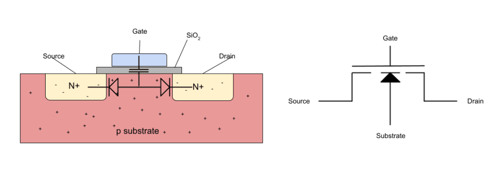
The gate terminal is a conducting plate separated from the P-type substrate by a thin insulating layer of SiO2. In effect, this makes a capacitor between the gate and the substrate.
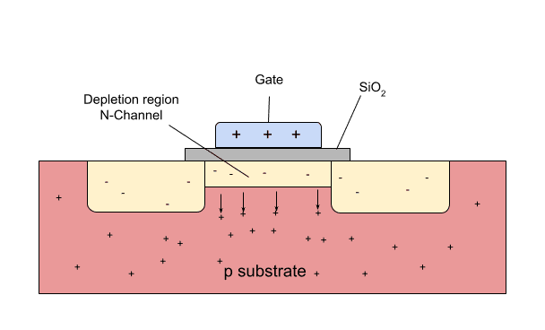
During operation, a positive potential difference is applied to the gate, relative to the substrate potential. This is usually held at the same potential as the source and therefore often referred to as VGS. The positive charge on the gate repels the positive charge carriers (holes) and attracts negative charge carriers (electrons) in the P-type substrate material immediately below the gate. The effect is to create an area that is depleted of positive charge carriers, called the depletion region, immediately below the gate. The depletion region now has an excess of electrons and is induced into being an N-type region, or N-Channel between the source and drain terminals. Electrons can flow through the N-Channel from source to drain, thereby creating a current through the device.
In a digital circuit, the gate potential is switched from rail to rail, resulting in the device being either completely off or completely on, with a fully depleted N-Channel. This fully depleted mode is called saturation.
In an analog circuit, the transistor is typically operated in the ohmic region, this is where the current that is allowed to flow through the device ID is proportional to VGS. To achieve this VGS operates in the range of potentials which result in a partially depleted N-Channel.
In the ohmic mode, the gain of the device is very sensitive to the potential difference between the gate and the substrate. A small change in the substrate potential has a large effect on the current through the device. To construct an analog MOSFET circuit that will work as required it is necessary to insert structures into the layout that carefully control the potential of the substrate.
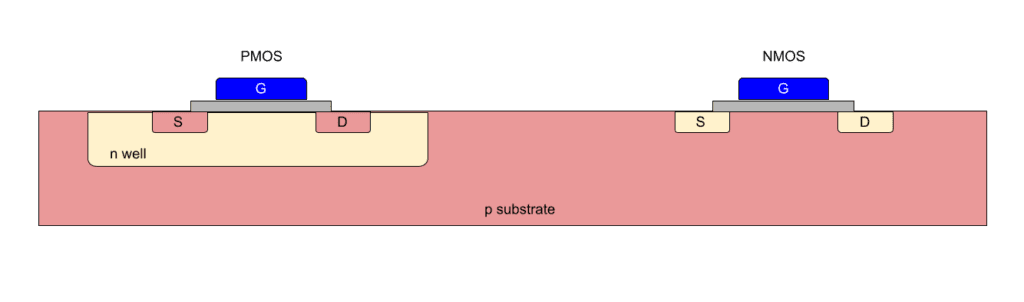
There are three main types of MOSFET devices that are used in the majority of processes. (we will leave SOI for another article). N-Channel devices in a P-type substrate (as above), P-Channel devices in an N-well, and N-Channel devices in what is called a deep N-well.
What is an N-well
Most processes are first doped to have a P-type substrate across the entire surface of the chip. So N-Channel devices can be built directly on top of this P-type substrate. P-Channel devices need an N-type substrate in which to form a P-type channel. To achieve this an area of N-type material is first deposited where P-Channel devices are going to be made. This N-type area is called an N-well.
What are taps?
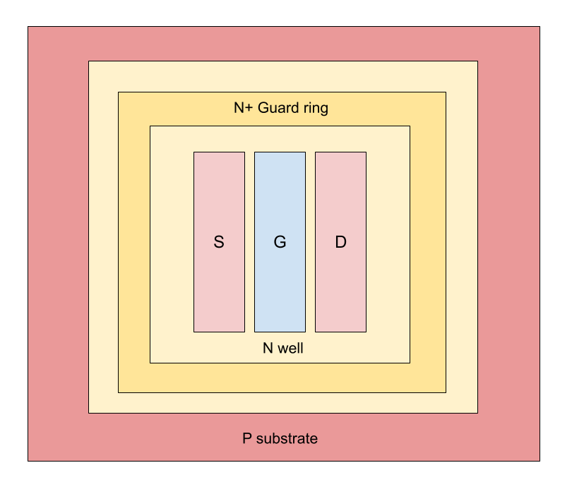
The N-well is effectively isolated from the other parts of the circuit, but during operation, charge can build up in the N-well. This charge changes the VGS of the P-Channel devices and thereby the performance of the circuit. To prevent this N+ “taps” are inserted into the layout that allows the charge to drain away and N-well to be held at the correct potential.
The N-type material in the well is fairly resistive, so to ensure good control of potential multiple taps are needed for each N-well spread throughout the area. In a similar way, P+ substrate taps are added to the P-type substrate to control charge build-up in the substrate. The process design rule manual (DRM) will specify a maximum distance between taps to avoid latch-up, but taps need to be inserted far more frequently to ensure good operation of an analog circuit.

What is a guard ring?
Most analog designs use an extended tap structure called a “guard ring”. Guard rings in analog design are large taps that completely enclose a group of devices. Guard rings more effectively isolate devices from each other, by creating a low resistance ring in the well/substrate around the group. This prevents charge buildup by other devices or fluctuating potential of other devices from affecting the operation of the guarded group.
How are guard rings used?
The guard ring shape is usually repeated in metal 1 and multiple contacts drawn connecting the metal 1 ring with the N+ ring. This ensures a good connection between the guard ring and (usually) power or ground. Increasing the width of the guard ring and the number of contacts further improves the isolation but at the expense of layout area.
Guard rings are particularly important in mixed-signal designs, where sensitive analog circuitry is located near “noisy” digital CMOS circuitry. Sometimes in particularly sensitive circuits, it is necessary to put every device in its own well, with its own guard ring, but in most cases devices in the same circuit can share the well. A common strategy is to create extra guard rings around certain parts of the circuit, e.g. a differential pair, giving it extra protection from its environment.
What is a Deep N-well
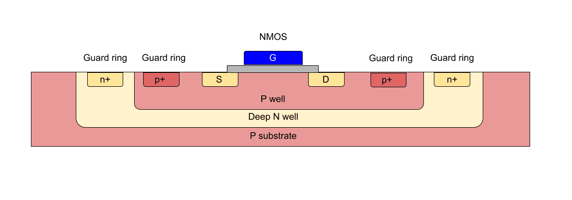
N-channel devices built directly into the P-type substrate are not as effectively isolated as P-Channel devices in their N-wells. This is because despite creating a P+ guard ring around the devices, there remains an electrical path below the guard ring for charge to flow. To overcome this issue a deep N-well can be used to more effectively isolate these N-channel devices.
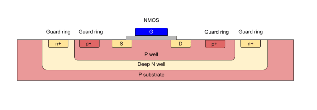
An N-well is constructed around and beneath (hence deep) the device’s P-Well. The N-channel device operates in the P-well. Both the P-well and the deep N-well need to be tapped, but in many cases, both wells are protected with guard rings. This means that the device has two rings around it, greatly improving the isolation of the device but requiring a great deal of space in the layout.
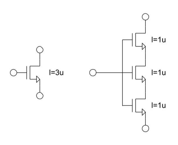
An added factor when designing wells, taps, and guard rings is their effect on device matching. Many analog structures, e.g. current mirror and differential pairs, require precise matching of the characteristics of different devices. A primary method of achieving good matching between two devices is to match their geometry as closely as possible. This extends to the wells, taps, and guards rings around them. A device placed close to a guard ring will have different characteristics to one placed further away.
For most designers, the layout geometry of the MOSFET is created by the pcell/pycell, but the position and geometry of the wells, taps, and guard rings are left to the expertise of the designer. DRC and LVS checks will, in most cases, tell the design where they have made mistakes, but these tools can’t measure the quality of the resulting layout. Expert layout designers should understand what these structures do, why they are needed and the effect they have on the circuit.