How big is my analog circuit?
Internet of Things (IoT) ICs are made from many functional units, digital logic, CPU, battery management, ROM, RAM, and many analog blocks DAC, ADC amplifiers, etc. IoT chips, such as MCUs, are complex system on chip (SOC) designs. Creating the right floorplan for the chip is a critical task that must evolve and be refined as the project progresses.
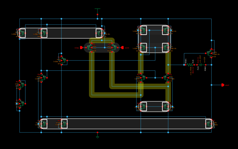
Some blocks, particularly random logic can be shaped to fit the available space, but others have fixed shapes. The floorplan is often constrained by the memory blocks with very predictable sizes and by the various analog circuits in the design. The shape and size of analog blocks are dictated by the performance requirements of the block, i.e. the need for device matching and LDE considerations, etc.
The floorplanning task starts almost as soon as work on the project is begun. The floorplan designer takes early circuit information and uses that to create the initial floorplan. This is usually done long before the layout of any functional block is available, and the designer relies on accurate estimations of block area and size. Getting accurate size estimations for analog blocks is critical to creating an initial floorplan because of the knock-on effect they have on the size and shape of many of the other blocks on the chip.
Unfortunately, area estimation is a notoriously hard problem among analog designers. Many people think that analog design area can’t be estimated for a circuit until you have completed its layout. But needing some sort of early estimate, many designers use rule-of-thumb methods of estimation. One commonly used rule of thumb is
Area Estimate = ( Active Area x 3.5 ) + Passive Area
So, how useful is this rule of thumb?
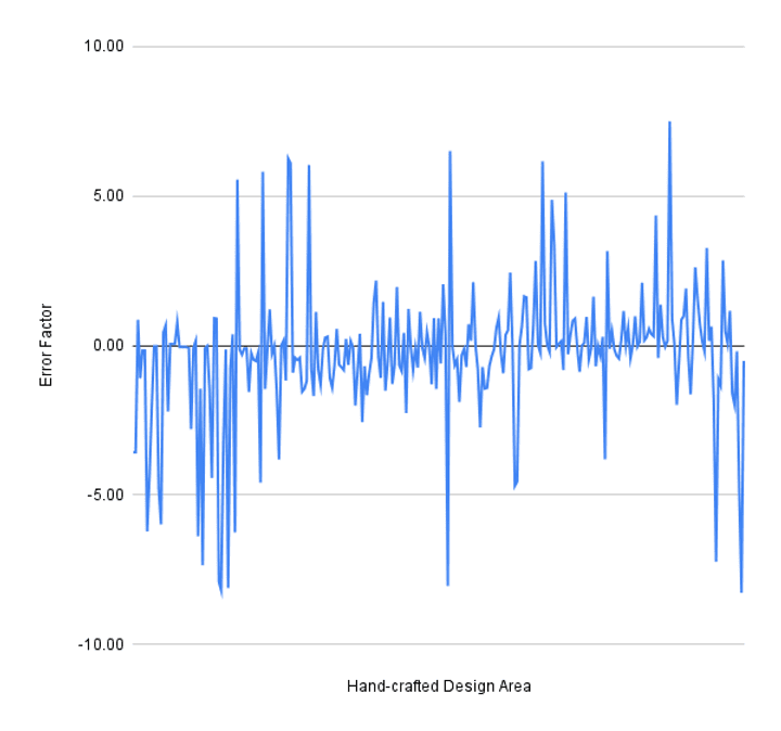
I was recently involved in some research [1] into various methods of analog area estimation. We looked at 280 different analog designs, targeting 13 different processes, from 0.6um to 28nm, across 7 different foundries. Using this data, we calculated the rule-of-thumb design area for every design and compared it against the actual handcrafted layout size in each case. The results were illuminating.


The chart above shows a plot of the error factors for the rule-of-thumb estimated areas. The error factor is a simple indicator of how many times too-large or too-small the estimate is compared to the handcrafted area. You can see that the estimate varied wildly, with some of the estimates off the mark by as much as 8x.
The analysis showed that the rule-of-thumb methods give very poor quality of design area estimation for analog designs. With a standard deviation in the error factor of 4.14, the rule-of-thumb method should not be relied upon to create accurate estimates for floorplanning. An SD of 4.14 means that many estimates range between 4x too large or 4x too small. This means that a 1:1 aspect ratio analog block might have horizontal and vertical dimensions 200% larger or smaller than the estimate provided. This low level of accuracy renders the estimates unusable, even early-stage floorplanning.


So what is the alternative?
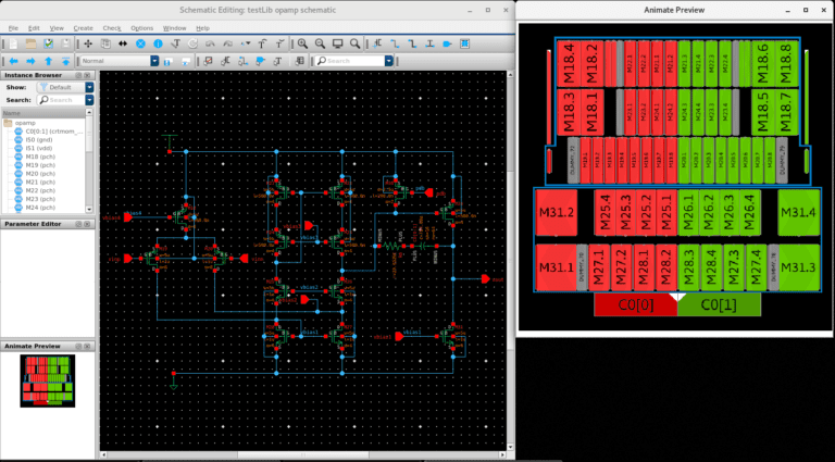
Instead of estimating the area of an analog circuit using a rule-of-thumb, an alternative approach is to use analog layout automation to create a layout. The research went on to compare the accuracy of the estimates given by the rule-of-thumb method against a newly available analog layout automation solution.
Using the same 280 real-world circuits, the following chart plots the estimation error factors when using analog layout automation over the top of the previous chart.


It is easy to see that the estimates from automation were much more accurate. Indeed, the standard deviation in error factor using automation was much smaller at 0.57, with most estimates are within 60% of the actual design size. Meaning that a 1:1 aspect ratio analog block would have horizontal and vertical dimensions within 25% of the estimate provided by automation.


This much-improved level of estimation accuracy can be obtained from the schematic, early in the design flow, and completely automatically, i.e. without a designer needing to create a trial layout. We can see that analog layout automation can now provide analog designers with estimates that are actually useful and can be used to create initial floorplans for their mixed-signal IoT silicon chips.
A fully automated, final-quality analog layout may not yet be a reality. But, recent advances in the state of the art mean that analog layout automation is starting to deliver useful features that can help analog design teams and chip floorplan designers.
References:
[1] M. Waller et al. Analog Integrated Circuit Design Area Estimation.

