Analog industry silicon foundries
Silicon foundries around the world
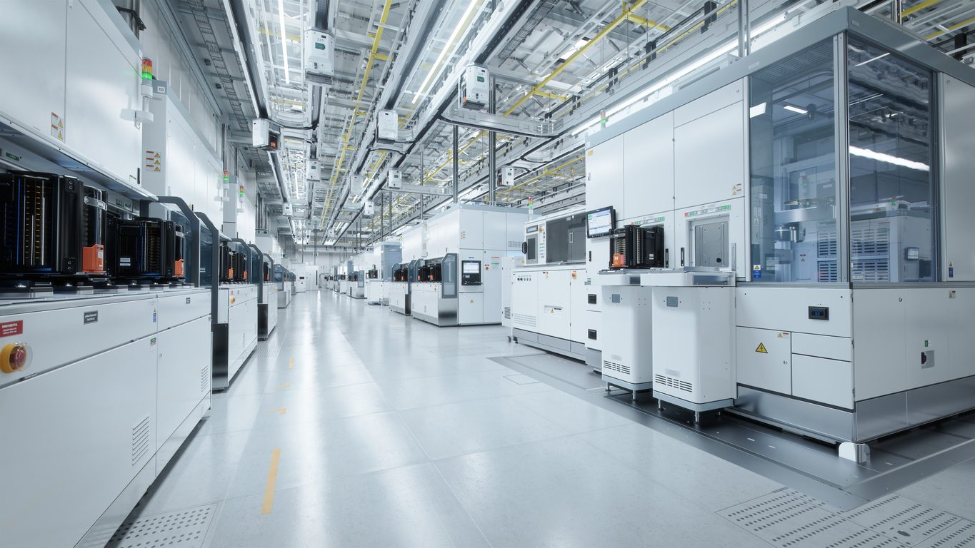
Silicon foundries play a crucial role in the electronics industry, as these foundries are responsible for turning the designs of integrated circuits (ICs) into physical chips that can be used in electronic devices. In this blog post, we will take a closer look at several major silicon foundries and their importance in the electronics industry.
The chip manufacturing industry has been a source of global tensions in recent years, with countries vying for control over the production and supply of these critical components. Chips are essential in modern technology and are used in almost every electronic device, from smartphones and laptops to military equipment and medical devices.

World’s largest silicon foundries
There are several major silicon foundries in the world that specialize in the production of analog chips, including:
- TSMC (Taiwan Semiconductor Manufacturing Company) – Based in Taiwan, TSMC is the largest foundry in the world and specializes in a wide range of technologies, including analog and mixed-signal processes. According to the Semiconductor Industry Association TSMC is responsible for around 55% of the chip production worldwide.
- GlobalFoundries – This company is based in the United States and operates several fabrication facilities around the world. They are one of the major players in the industry, with a focus on advanced technologies for analog, mixed-signal, and RF applications.
- UMC (United Microelectronics Corporation) – Another Taiwan-based foundry, UMC specializes in a wide range of technologies, including advanced analog and mixed-signal processes.
- SMIC (Semiconductor Manufacturing International Corporation) – Based in China, SMIC is one of the largest foundries in the world and offers a wide range of technologies, including advanced analog and mixed-signal processes.
- ASE (Advanced Semiconductor Engineering) – Headquartered in Taiwan, ASE is a leading provider of analog and mixed-signal IC packaging and test services for a wide range of applications, including automotive, communications, consumer, and industrial.
TSMC: A key player
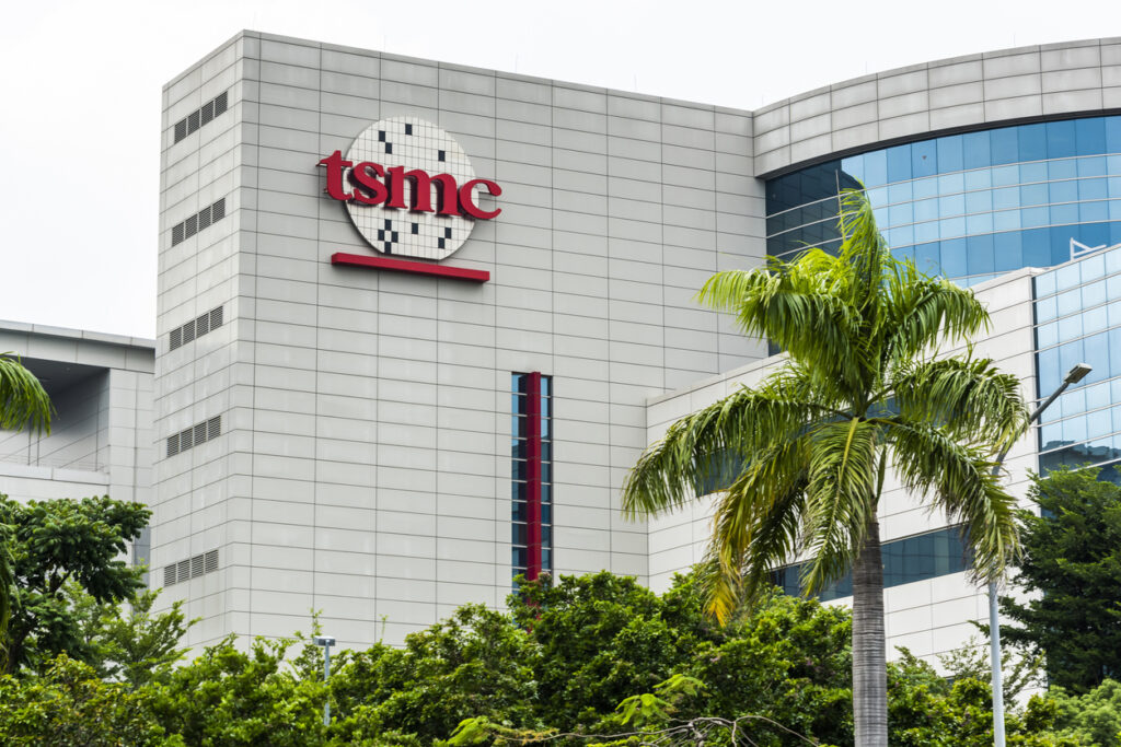
One of the largest silicon foundries in the world is TSMC (Taiwan Semiconductor Manufacturing Company). Based in Taiwan, TSMC is the largest foundry in the world and specializes in a wide range of technologies, including analog and mixed-signal processes. They are known for their advanced process technologies and are considered a leader in the industry.
At present, TSMC has majority of the global market for contract chip fabrication and has its specific fabrication rules. These rules or set of files model the design process to design integrated circuits. They are called Process Design Kits or PDK’s.
In December 2022, the company announced the creation of their first fab in Arizona, USA. These new facilities will allow the production of N4 processes in 2024 and could begin the production of 3nm process technology in 2026.
Why are PDK’s important?
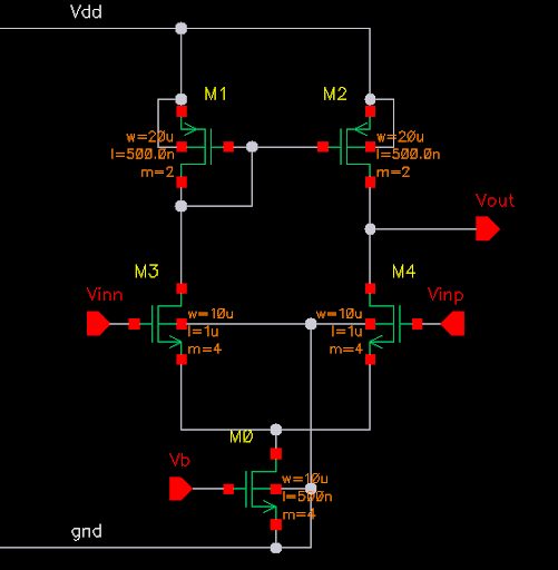
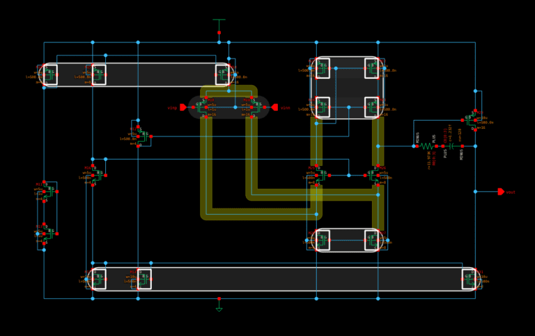
Since PDK’s can be different from one foundry to another, analog designers need to be aware of them as they are critical to prevent faults in the integrated circuits. Each foundry defines a certain technology variation for their processes. It is then passed to their customers to use in the design process. The customers may enhance the PDK, tailoring it to their specific design styles and markets. The designers use the PDK to design, simulate, draw and verify the design before handing the design back to the foundry to produce chips. The accuracy of the PDK during the design process is paramount to increase the chances of first-pass successful silicon.
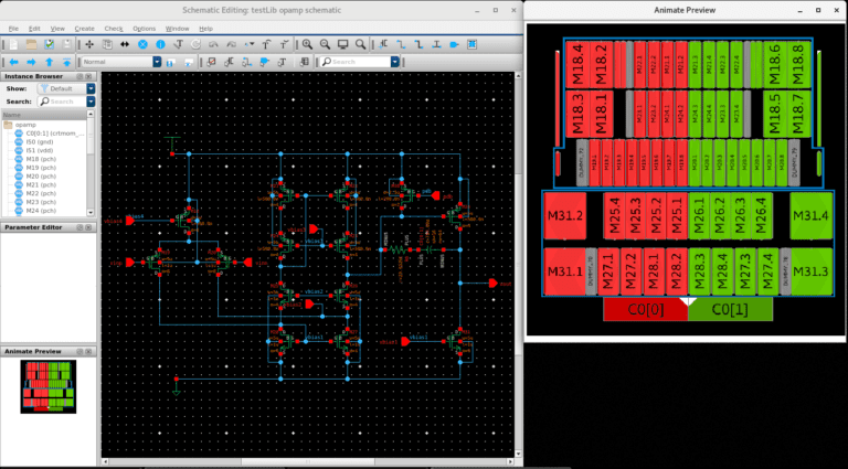
DRC rules on Animate Preview
Animate ensures great results for TSMC processes from 180nm down to 22nm. However, Animate will work with any planar process on OpenAccess with Cadence P-Cells. We have customers using Animate on many other processes from several fabs. We’re also starting to support some FD-SOI technology. At the moment FinFET is not supported (14nm, 10nm, 7nm, 5nm, and smaller nodes.)
Once loaded or modified, the resulting IC layout will be DRC clean, especially for TSMC processes. For other processes, if the rules are in the Open Access tech file, Animate will obey them. Most customers get good results out of the box, but if a user has any issues, they can contact Pulsic for better support.
Would you like to try Animate Preview? Get your download link here: