Current Mirrors in Analog Layout
Current mirrors are found in almost every analog IC circuit to provide bias currents, current steering, and active loads. They are designed to copy (or mirror) the current flowing through a reference branch to one or more mirrored branches. Current mirrors are so widely used they are possibly the single most important building blocks of analog IC circuits, and often the first part of a circuit to be designed and laid out.
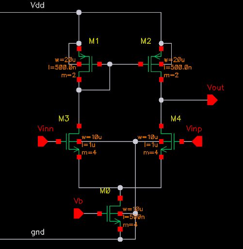
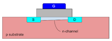
Let’s look at one typical example of a MOS current mirror in use.
In the circuit above the mirror is an active current load for the differential pair below it. In this type of circuit, it is essential that the loads on M3 and M4 are precisely balanced. Any mismatch in the current through M1 and M2 will skew the circuit and result in poor performance and the circuit not meeting specifications. This circuit and variations of it appear again and again in analog circuitry.
It is easy to draw a circuit schematic with matched devices for M1 and M2, but much harder to achieve when translated to silicon. MOSFET process variability means that two devices can not be guaranteed to match sufficiently. Variation across the die in doping/implantation density, oxide thickness, and many other causes lead to mismatched devices.
Variation in device oxide thickness.
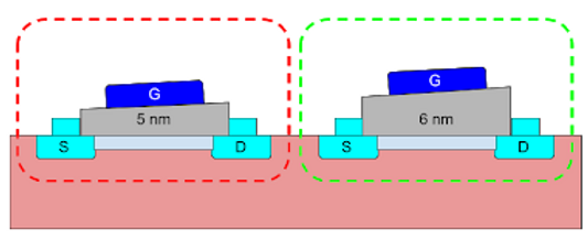
As current flows through an operating MOSFET, its channel depth varies across the length of the channel (causing pinch-off at saturation). The interaction between this effect and implant direction creates additional variation in device performance.
Variation in channel thickness.
Optical effects mean that “identical” devices, in reality, have different dimensions, and at process nodes below 40nm layout dependent effects (LDE) mean that the relative placement of devices affects their performance. An example of an LDE is the proximity of devices to the well edges. The distance of devices from a well edge has an effect on the Vt (threshold voltage) of the device. The cause is implant ions scattering off the resist sidewall used to define the well, thus increasing Vt by several, or even tens, of millivolts. (Faricelli, 2010)

Illustration of how Vt varies with distance from the edge of the well.
Circuit engineers and layout designers are aware of these issues when matching devices in current mirrors. One method is to use is Pelgrom’s law and make devices bigger. (Pelgrom et al, 1999) This improves Vt matching and noise performance, but at a cost of increased area and reduced bandwidth. Another is to match devices geometrically.
The devices in a current mirror should be drawn so that the geometry of each device matches as much as possible. Designers generally avoid matching devices with different parameterizations. e.g. 4 um width matching with 2 x 2 um width. While on paper they are still matched, i.e. same total width, in practice, this would result in a very poor match. For good matching, devices should be rotated the same way; several process effects, including implant direction, change the characteristics of differently oriented devices.
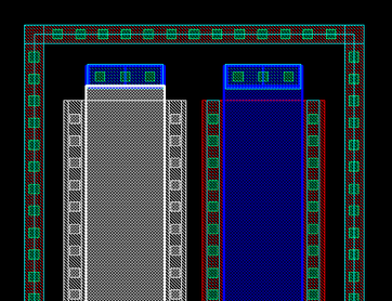
Matched layout with the reference device highlighted on the left.
Ensuring that the two branches of the current mirror have identical parameterized devices is essential. Similarly, the layout immediately around each of the devices needs to match, e.g. proximity to other devices and guards rings, etc.
The next strategy is symmetry, splitting each device into multiple smaller devices and placing them on either side of a line of symmetry. The reference device is usually placed in the center and the other device split around it. Placing the reference device in the center is more important in current mirrors with more than one bias device, where engineers need to match multiple MOSFETs, but is also common practice in simple mirrors.
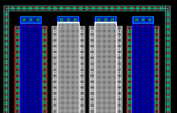
Common centroid layout with the reference device in the center.
This common centroid design style improves matching by averaging out the effect of variation in the process.

Common centroid design evens out the effect of the process variation.
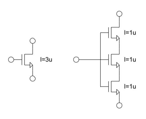
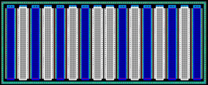
Splitting the mirror devices into a larger number, each with a smaller width also improves matching, as process variations and optical effects are “averaged out” across a greater number of devices.
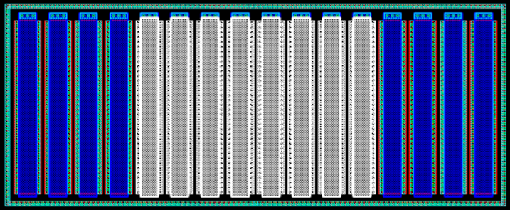
Common centroid design with a larger number of devices.
In the above diagram you can see the same current mirror, but each device has a width of only 5u instead of 20u, the total width of each device is the same as before, but the overall matching between devices will be better.
An alternative common centroid pattern is called maximum dispersion. In this pattern, the two devices are still placed in a common centroid pattern but are also interleaved. This can also improve device matching further as it can help even out some LDE effects; however, this does make routing more complex and increases design area.
Maximum dispersion layout style.
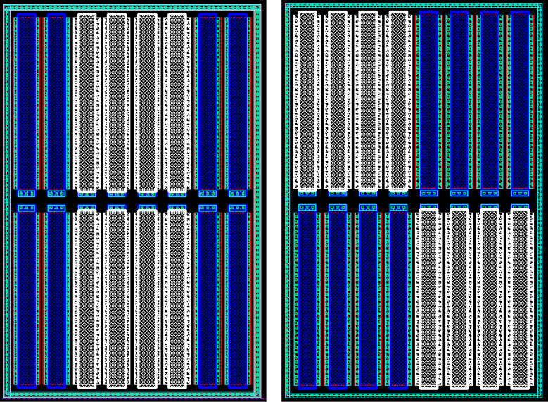
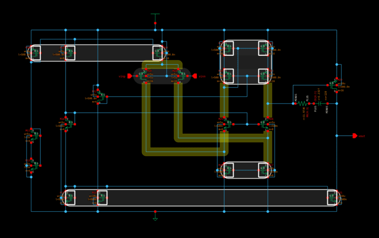
Two-row current mirror. Simple routing on the left and cross-quad on the right.
For large devices it is common to arrange the mirror across 2 rows, either to fit the available space or improve matching by bringing the devices closer together, reducing the likely variation across the current mirror. The reference in the center pattern, on left in the images above, is simpler to route. The “cross quad” pattern, on the right, is used to further improve tolerance to across die variation in any direction but is more complex to route as it requires the routing to cross over in the center.

Source contacts highlighted to show current direction.
As mentioned earlier, the current direction through the device also matters. It is common to flip the current direction around the line of symmetry. In the above case, the source of each MOSFET is highlighted, and you can see that they are symmetrical about the center of the image. This simplifies the routing process, making it easier to achieve symmetrical routing, but this may be at the expense of device matching due to the channel thickness effect, discussed above.
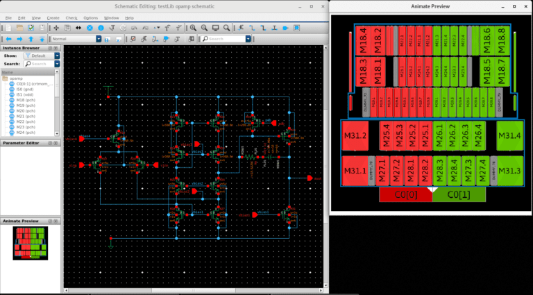
There is often no “right” answer in analog layout. All analog layouts are necessarily a compromise between multiple competing requirements; matching, isolation, design area and aspect ratio, routing, and much more. Circuit engineers and layout designers use their knowledge and experience to choose the right set of compromises for their design. Pulsic’s Animate Preview automatically chooses from all the techniques discussed in an intelligent way to create a layout preview of your design in seconds, reducing design iterations. Visit https://animate.pulsic.com to learn more.
The techniques discussed in this article are just the starting point for achieving good MOSFET matching in current mirrors. For example, modern processes demand that the designer also insert dummy devices and consider device density. These are the topic of my next blog post.
References:
J. V. Faricelli, “Layout-dependent proximity effects in deep nanoscale CMOS,” IEEE Custom Integrated Circuits Conference 2010, San Jose, CA, USA, 2010, pp. 1-8, doi: 10.1109/CICC.2010.5617407.
Pelgrom, M.J.M. & Tuinhout, Hans & Vertregt, Maarten. (1999). Transistor matching in analog CMOS applications. Technical Digest – International Electron Devices Meeting. 915 – 918. 10.1109/IEDM.1998.746503.